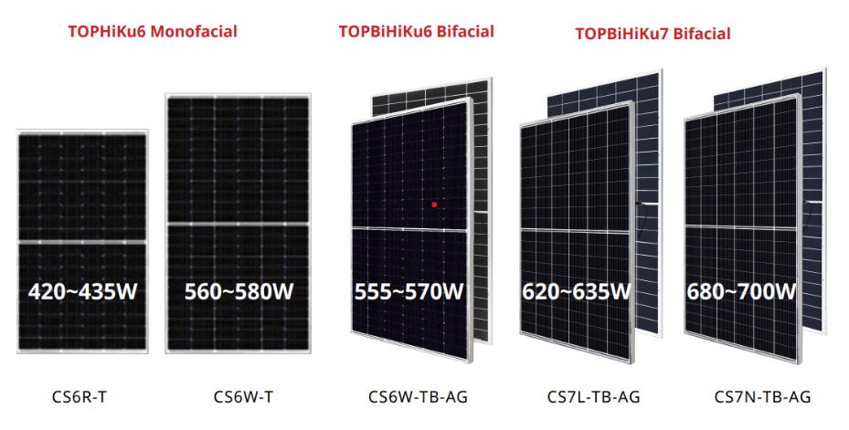
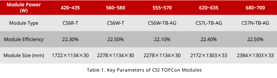
Canadian Solar was one of the first companies to introduce PV cell and module technologies that later became the industry mainstream, such as bifacial modules (back in 2010), modules with larger-format wafers (up to 210 mm) and, nowadays, N-type high-efficiency cells and modules. Since 2019, CSI Solar has been developing N-type TOPCon (Tunnel Oxide Passivated Contacts) technologies, and is now launching a diversified TOPCon module portfolio covering both 182 mm and 210 mm cells, single-glass and double-glass encapsulation, and various module sizes and power outputs to satisfy different application scenarios.
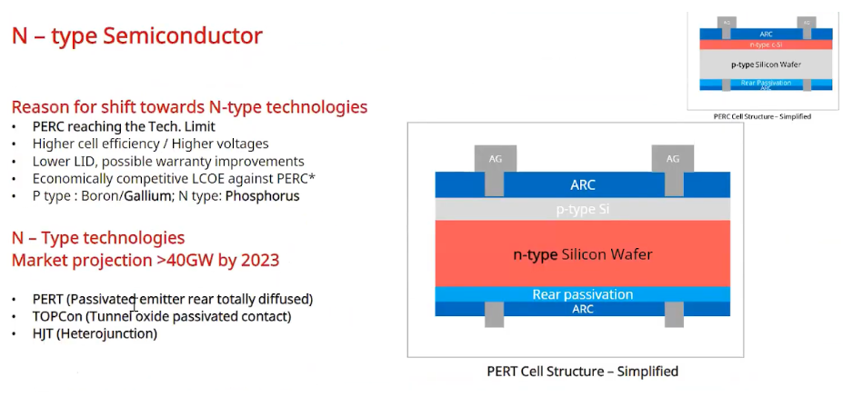
N-type silicon is a type of semiconductor material that has different doping characteristics compared to the more commonly used p-type silicon. N-type silicon offers several advantages, including lower sensitivity to light-induced degradation (LID) and better temperature coefficients, resulting in improved performance and durability.
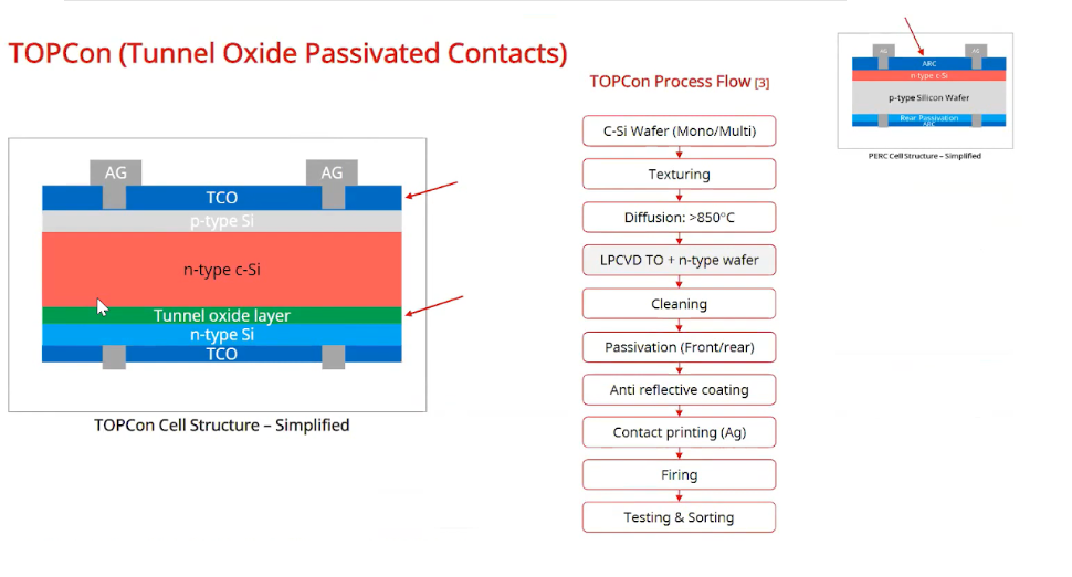
TopCon technology, on the other hand, utilizes a thin layer of silicon oxide to passivate the surfaces of the solar cell, reducing carrier recombination and improving overall efficiency. This technology helps to achieve higher energy conversion efficiency by minimizing energy losses.
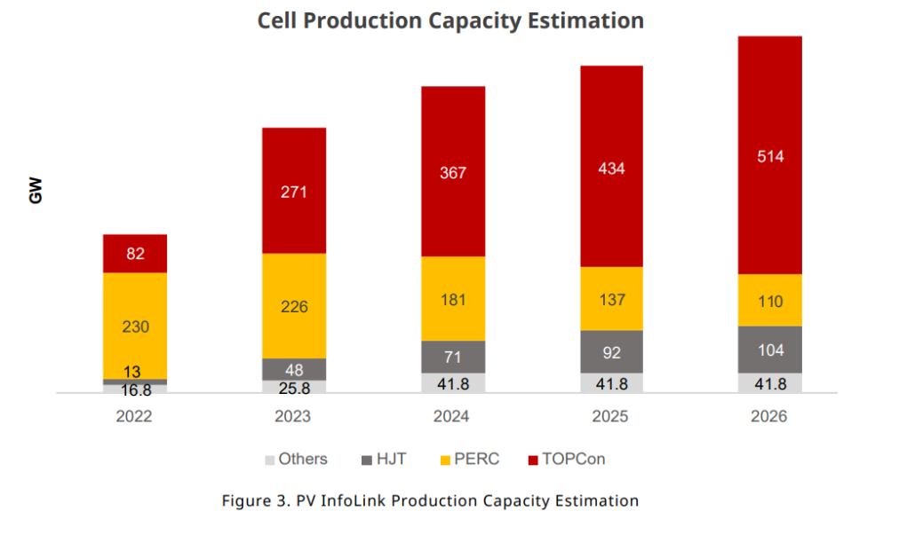
When combined with N-type silicon wafers, the upper efficiency limit of TOPCon cells is estimated to be 28.7%, outclassing that of PERC, which would be about 24.5%. TOPCon’s processing is more compatible to the existing PERC production lines, thus balancing better manufacturing cost and higher module efficiency. TOPCon is expected to be mainstream cell technology in the coming years.
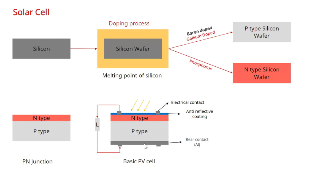
Solar cell construction
A PV cell is basically composed of two layers, a base layer and an upper layer. Boron or gallium are the dopants utilized in p-type doping. Each of the outer orbitals of these elements contains three electrons. They create ‘holes’ in the valence band of silicon atoms when they are incorporated into the silicon lattice. As a result, the valence band’s electrons become mobile and the holes migrate in the opposite direction of the electrons. Only the positive charges are free to migrate since the dopant is fixed in the crystal lattice. These semiconductors are referred to as “p-type” (or “p-conductive” or “p-doped”) because of the positive holes.
N-type solar cells have a slightly different construction compared to traditional p-type solar cells. The main difference lies in the doping of the semiconductor material used in the cell.
Here is a general overview of the construction of an n-type solar cell:
Substrate: The solar cell starts with a substrate, which is typically a thin wafer made of high-purity monocrystalline or multicrystalline silicon.
N-type Dopant: The front side of the substrate is doped with an n-type dopant, such as phosphorus. This introduces extra electrons into the silicon lattice, creating an excess of negatively charged carriers.
Anti-Reflective Coating: A thin layer of an anti-reflective coating, such as silicon nitride (SiNx), is deposited on the front surface of the cell. This coating reduces reflection losses and enhances light absorption.
Front Metal Contacts: Metal contacts, typically made of silver or silver/aluminum paste, are applied to the front surface to collect the electrons generated when sunlight hits the cell. These contacts are arranged in a grid-like pattern to maximize the collection area.
Passivation Layer: A passivation layer is applied to the front surface to reduce recombination of charge carriers. This layer is usually made of silicon oxide (SiOx) or a combination of silicon oxide and silicon nitride.
Back Metal Contacts: On the back surface of the cell, a metal contact is applied to collect the positive charge carriers (holes) created during solar cell operation. This back contact can be a full-area aluminum layer or a patterned design.
Back Surface Field: To further enhance cell performance, an additional layer known as the back surface field (BSF) may be included. This layer, usually made of heavily doped silicon, helps to create a gradient in the electric field, facilitating the efficient collection of charge carriers.
It’s important to note that the actual construction details may vary among different manufacturers and specific cell designs. The above description provides a general outline of the construction process for n-type solar cells.
N-type Topcon and Hetrojunction PV cell structure
The structure is compatible with both p- and n-type wafers and can theoretically be applied to either side of the wafer. However, when doped polycrystalline is utilized on the front side, it leads to greater absorption losses since polysilicon has a similar band gap to crystalline silicon. While there are ways to avoid losses from unwanted absorption, they are not yet suitable for production since they require intricate masking and etching procedures. As a result, the term “passivated contacts” is primarily used in the industry to refer to the back side engineering.
Due to this, the bulk of the industry still uses passivated contacts on the back of n-type wafers, despite the fact that researchers are also working on p-type passivated contact cells. One such research institute is the German Solar Research Institute ISFH, who recently demonstrated their method.
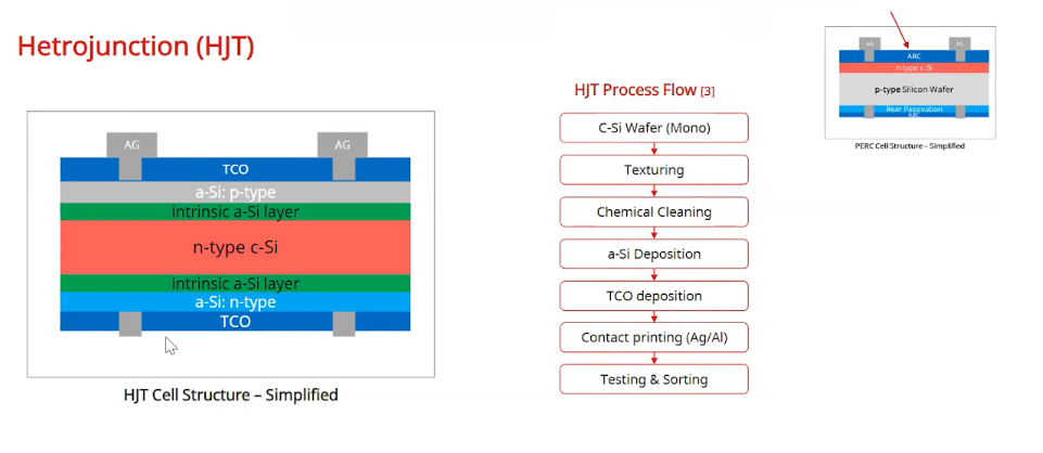
Heterojunction solar cells combine two different technologies into one cell: a crystalline silicon cell sandwiched between two layers of amorphous “thin-film” silicon. This allows an increase in the efficiency of the panels and more energy to be harvested easily when compared to conventional silicon solar panels. The most common type of solar panel is made with crystalline silicon – either monocrystalline or polycrystalline. Amorphous silicon is thin-film silicon unlike crystalline silicon, amorphous silicon does not have a regular crystalline structure. Instead, the silicon atoms are randomly ordered. As a result, manufacturing this type of solar cell is less expensive.
This lower cost and flexibility in the type of materials that amorphous silicon can be deposited on are a couple of important advantages. With heterojunction solar cells, a conventional crystalline silicon wafer has amorphous silicon deposited on its front and back surfaces. This results in a couple of layers of thin-film solar that absorb extra photons which would otherwise not get captured by the middle crystalline silicon wafer. The HJT production concept was developed by SANYO Electric in the 1980s (SANYO was acquired by Panasonic in 2009). SANYO was the first company to commercially produce solar cells made of amorphous silicon. Heterojunction solar technology takes advantage of this by building a solar panel out of three different layers of photovoltaic material.
The top and bottom layer are made up of thin-film amorphous solar cells, the middle layer is a crystalline solar cell. The thin-film silicon on top captures some sunlight before it hits the crystalline layer, and it also grabs some sunlight that reflects off the layers below. It’s very thin, so much of the sunlight passes right through and the sunlight that passes through the middle, i.e the crystalline layer, is absorbed by the thin amorphous layer that is below. By building a panel out of a sandwich of three different photovoltaic layers, a heterojunction solar panel can reach efficiencies of 21% or higher. This is comparable to panels that use different technologies to achieve high performance.
Comparison between PERC, Topcon and Hetrojunction modules
Solarity availability of new Topcon modules
Solarity has secured a decent quantity of Topcon N-type modules in the warehouse. Currently, Solarity can provide the market with 565W bifacial Topcon modules as this power class is in the most demand on the market. Also, Solarity will soon secure a higher power class of Topcon modules for C&I projects, either in regular or bifacial types. The power class will be 656 W and above as Canadian Solar will provide up to 690 W modules.